Another way how to drive TC is using semiconductor parts. Usually the bridge circuit
with power MOSFETs is used. But semiconductors are so fragile. They dislike (short) high-voltage/current peaks.
And the capacitive current to gate is quite big at frequencies about 1 MHz. Gate capacity of usual power MOSFETs
is about 2 - 10 nF. This means that we need power gate driving circuit which is able to source/sink
several amps to/from gate electrode during peaks. They are manufactured as integrated circuits but it's hard to buy
them in Czech Republic. Sometimes when I'm buying electronic parts it seems that I'm living in Africa ;-). Our professors
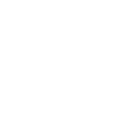
on our eltech. faculty (of Czech Technical University) show us (in subject Theory of electromagnetic field 1) a small TC
powered by single transistor self-oscillating driver. Thanks to prof. Pankrác who allowed me to explore the SSTC driver PCB
and draw schematic - here is it:
SU169 is high-voltage switching transistor from deflection circuit used in old B/W TV. Its max. parameters are:
UCB0 = 1000 V, UCE0 = 400V, IC = 10 A, UEB0 = 8V, Ptot = 100 W,
h21E >=15. Diodes may be some generic rectifier 1000V / 1A, faster are better. I built it at home on
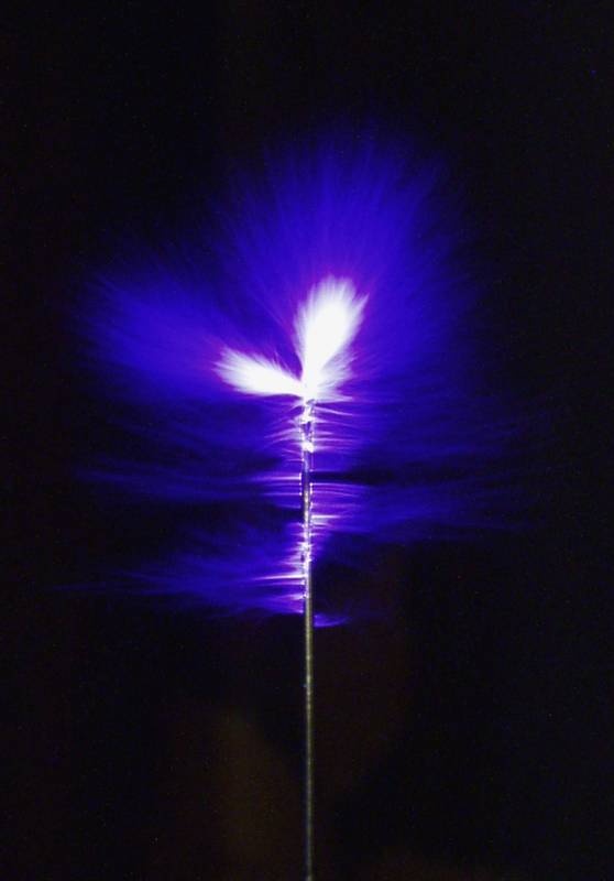
a small PCB and it worked on first light. It draws about 1,5 A at 35 VDC and do about 2 cm sparks with
quiet hissing noise like HV from TV. When I applied higher voltage to driver the sparks become longer but only for a while.
After few second the transistor "pops" breakdown and game over. I tried to use other transistors such as SU161,
BU208... but they died too. Usually the junction B-E was shorted and junction B-C blown up. I have only old
oscilloscope Křižík (assembly date about 1950 :-) which can't displays short voltage peaks or other evils damaging
my transistors. Here is some photos of my SSTC driver on PCB.
And here how it works:
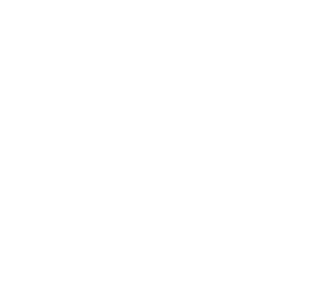
MOSFET flyback
26.9.2002 I was thinking about usage of power
MOSFETs to driving tesla coil for a long time. Bridge circuits seems too complicated to me. This is because
driving a high-capacity FET's gates is not easy at high frequencies about 1 MHz. I have an idea to
replace vacuum tube by FET in my VTTC flyback driver. I found an IRF640 (200 V; 18 A; 125 W;
0,18 Ω) FET in my stock. Voltage from feedback coil is clamped with two Zener-diodes KZZ75 to
protect gate (I know that it is not optimal solution). I powered the circuit from variac (half-wave
rectified and filtered by 100 µF capacitor). To start the circuit oscillating a short connection
of gate on positive voltage via hi-ohm resistor is needed. Then I connected resistor to ground to prevent
FET damage if oscillations drops out and FET would remains opened. This will need better solution. When I
powered it by smoothed 70 VDC I got sparks like with SU169 BJT driver (on my big TC).
Then I reconnected it to variac half-wave rectified output. This made
sparks like PL504 VTTC driver at about 120 VAC. And there's no serious
cooling problem. When I applied higher voltage FET popped. I'm planing parallel connection of about four
IRF740 or IRF840 powered directly by rectified mains. It will simplify the power supply for the driver
and make it smaller.
MOSFET half-bridge I
14.5.2003 After IRF640 has died in my MOSFET
flyback I tried to replace it by parallel combination of IRF740 and other MOSFETs but with no result. The
circuit won't start to oscillate in any case (nor with IRF640 originally used). I checked and replaced
everything that I can but the circuit was never started oscillating like before.
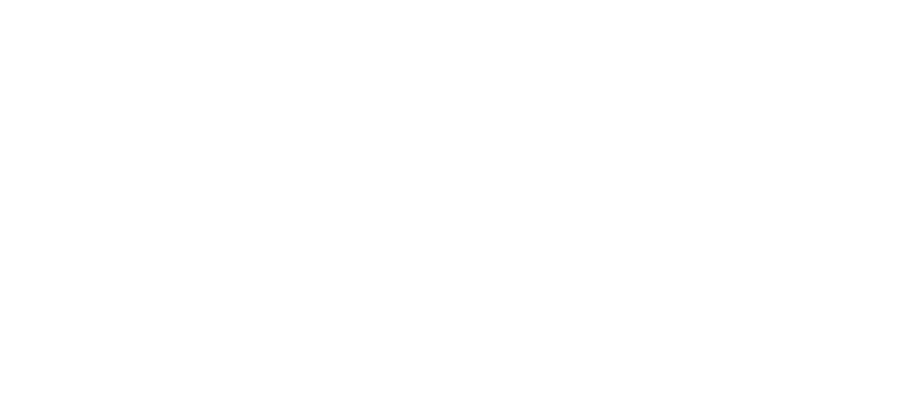
I successfully obtained two samples of MAX5048
integrated circuit via Internet. It has especially developed for driving power MOSFETs. It's incredible
how this IC in tiny SMD package can handle 7,2 A peak current to gate. I tried to drive a common
5 nF capacitor. At 1 MHz the waveform was still looking quite good but circuit and capacitor
was heating. With this ICs I finally could start to build my own MOSFET half-bridge. The half-bridge behaves
like an electronic alteration switch which alternately connects the load to +Ucc rail and ground rail.
The major advantage of half-bridge compared to flyback is that half-bridge has better efficiency and limits
Uds across MOSFETs to maximum of +Ucc rail voltage. It has also a disadvantage - danger of simultaneous MOSFETs
conducting called cross-conduction or shoot-through condition which cause immediate MOSFETs damage.
The first problem needed to be solved was driving the high-side MOSFET. It's gate
floats at high voltage level and cannot be connected to MAX IC directly. So I decided to use insulating transformer
called GDT - Gate Driver Transformer. The GDT requires high quality magnetic core (low RF losses by eddy currents).
Also it needs to be trifilar wounded to get high coupling coefficient. It has limited bandwidth excluding DC and too
low or high frequencies. And output DC bias depends on input duty cycle. But this doesn't matter when we use it
for driving a tesla coil which has very narrow bandwidth and needs 50% duty cycle. In other hand there's a lot of
advantages:
1) galvanic insulation of GDT windings (also protects the driver when MOSFETs fails)
2) easy phase shift of 180° by simple swap of winding leads
3) GDT may have more windings (one GDT for full-bridge)
4) transformation ratio can be other than 1:1
5) when any driving signal present both MOSFETs have shorted gates and are closed
6) zero DC bias with 50% duty cycle cause symmetrical ±gate voltage (gain noise immunity,
reduction of cross-conduction while switching).
More details how to make a good GDT you will find in this design guide.
Now I try to explain why so big gate currents are needed for power MOSFET's driving.
FET means Field Effected Transistor - transistor driven by (electric) field.
This evoke impression that there's no currents and no energy is needed for driving but this is a mistake.
Any chick paws for free ;-). By principle of MOSFET there's always some capacitance between gate-source and
gate-drain. And this capacitance is not insignificant small in power MOSFETs. IRF640 has Cg about 2,5 nF and total
gate charge 67 nC. On every turn on/off the Cg has to be charged/discharged from supply of driving signal.
This effect is insignificant while switching frequency is low. But I need to operate my half-bridge at 1,2 MHz
(0,8 µs period). For reasonable losses MOSFETs should switch 10-times faster. It requires that signal supply,
with output impedance R, charges the gate in tau = 0,08 µs up to 10 V. So R value must be
about R = tau / Cg = 30 Ω. When gate is totally discharged it behaves like
short circuit and through 30Ω resistor will flow 0,5 A peak current from 15 V supply. Of course the
RMS current is much smaller. For faster MOSFET switch on is lower R and higher peak current to gate needed.
Semiconductor manufacturers offers integrated drivers with peak current up to 12 A and switching times about
40 ns nowadays. The capacity gate-drain is significantly smaller but more problematical. It causes
Miller's effect - transmission from output to input. When lower MOSFET turn off quickly voltage on its drain
rises quickly to +Ucc rail voltage. This make a pulse which is transfered via mentioned capacitance back to
gate. It may cause MOSFET's turn on again or its damage (common power MOSFETs have max. Ugs = ±20V).
Therefore we need signal supply with low output impedance which minimize influence of reverse transmission.
Also it's good idea to put some limiter between gate and source like two antiserial wired Zener diodes
which clamps Ugs to max. ±Zener voltage of this diodes and protects MOSFETs.
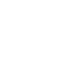 Another problem is how to eliminate MOSFET body diode - it is a diode "connected" between drain and source
(in N-channel anode to source, in P-channel cathode to source; usually not drawn in schematic sign).
This diode, which we got for a free from manufacturer, is given by manufacturing technology and cannot be removed.
It's useful as free wheeling diode for low frequency application but causes problems at higher frequencies.
It's reverse recovery time is much times longer than switching times of MOSFET itself. For example IRF640
body diode has trr = 170 ns and MOSFET's turn off time (tfall + toffdly) is 30 ns.
We can eliminate the body diode when we don't allow to open it. (When inductive load is turned off there
always flow some current back to supply; we must make some path for it - free wheeling diodes instead it
damages our MOSFETs). For this purpose we connect fast Schottky diode between drain and source. Schottky
diode has lower threshold voltage and opens sooner than body-diode could. But Schottky diodes usually
have low reverse voltage allowed. So we connect some common diode in series with MOSFET which increases
total forward voltage droop and then we connect a fast diode parallel to this combination as is shown on
left picture. If we didn't eliminate the body diode it causes that MOSFET stays opened after turn off due
to long body-diode trr. When opposite MOSFET turns on it make a shorted circuit. Big (cross)current will
flow from +Ucc rail to ground via both MOSFETs and it may shoot them out of your board. The SSTC theory
is very detailed described on
Richie Burnett's website. I recommend to read it.
Another problem is how to eliminate MOSFET body diode - it is a diode "connected" between drain and source
(in N-channel anode to source, in P-channel cathode to source; usually not drawn in schematic sign).
This diode, which we got for a free from manufacturer, is given by manufacturing technology and cannot be removed.
It's useful as free wheeling diode for low frequency application but causes problems at higher frequencies.
It's reverse recovery time is much times longer than switching times of MOSFET itself. For example IRF640
body diode has trr = 170 ns and MOSFET's turn off time (tfall + toffdly) is 30 ns.
We can eliminate the body diode when we don't allow to open it. (When inductive load is turned off there
always flow some current back to supply; we must make some path for it - free wheeling diodes instead it
damages our MOSFETs). For this purpose we connect fast Schottky diode between drain and source. Schottky
diode has lower threshold voltage and opens sooner than body-diode could. But Schottky diodes usually
have low reverse voltage allowed. So we connect some common diode in series with MOSFET which increases
total forward voltage droop and then we connect a fast diode parallel to this combination as is shown on
left picture. If we didn't eliminate the body diode it causes that MOSFET stays opened after turn off due
to long body-diode trr. When opposite MOSFET turns on it make a shorted circuit. Big (cross)current will
flow from +Ucc rail to ground via both MOSFETs and it may shoot them out of your board. The SSTC theory
is very detailed described on
Richie Burnett's website. I recommend to read it.
Here I used two MAX5048 drivers which works in full-bridge. This gives me ±12V
voltage amplitude on secondary side of GDT with 1:1 transformation ratio. I could use only one driver and
GDT with 1:2 transformation ratio but this will 4-times increases the output impedance (impedances are transformed
via square of transformation ratio). GDT primary is DC separated by capacitor. It's not needed for 50% duty cycle
when DC bias is zero. But it's very useful for drivers protection when clock signal is lost. If it would happen
one driver's output stays at High and other at Low and flowing DC current will damage them. I recommend to fuse
the drivers voltage supply to protect them. 75451 circuit works like TTL->CMOS converter and "deadtime controller".
It's purpose is prevent to overlay both driving signal using very shot delay while both signals are Low and both
MOSFETs are in off state. Using capacitor-trimmer you can vary the delay in some tens of nanoseconds. In practical
view the deadtime doesn't approved after connecting MOSFETs. Gate voltage curve has been smoothed. So I don't know
may be using of inverting and non-inverting MAX's input to generate both signals would be good enough.
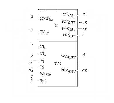
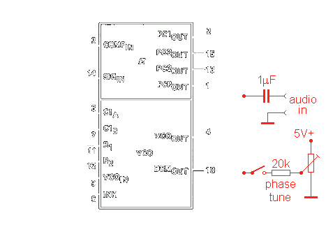
For synchronization with TC I used PLL circuit 74HCT4046. It is set (via R1, R2, C1)
to generate frequency around 1,2 MHz without any input signal. After TC is partially excited at it's natural resonating
frequency it induces some feedback signal to antenna of PLL circuit. PLL will lock at this frequency. When secondary
frequency changes PLL will automatically retune to serve right frequency. Input of PLL is protected with two clamping
diodes against too high input voltage. As an antenna I use few centimeters of wire or connection at one lead of
feedback coil via resistor.
Here are some oscillograms showing waveforms in interesting nodes. I used for this
job my new two channel oscilloscope Grundig MO 52
(it really couldn't be measured on my old Křižík scope from 50' :-). Time resolution is 0,2 µs/cm in all graphs.
 |
 |
 |
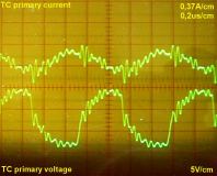 |
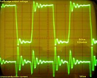
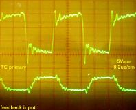
| Ug1, Ug2 |
Uout, Icross |
Uout, Uin |
Uout, Ipri |
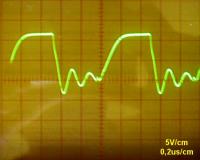
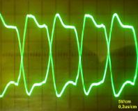
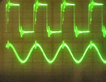
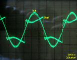
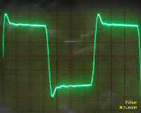
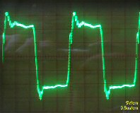
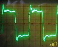
On 1st oscillogram you can see driving voltage at gates of both MOSFETs. This is nothing beautiful but designing a driver
at 1,2 MHz is a real nightmare. I tested it with simple generator which cannot give 50% duty cycle. On 2nd one is displayed
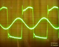
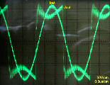
output voltage (which looks quite well) from half-bridge and supply current (with no load). So some cross-current is flowing.
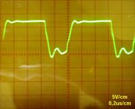
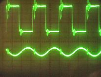
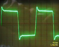
On 3rd one is output voltage from half-bridge and input voltage captured by antenna at PLL input. And on 4th one is current
flowing to primary coil and half-bridge output voltage. There's some ringing due to long wires which I used for testing.
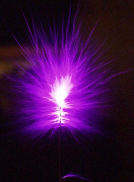
I tested with 70 VDC power supply and I got 3 - 4 cm spark length. Sparks
was very hot and melted my needle discharge electrode.
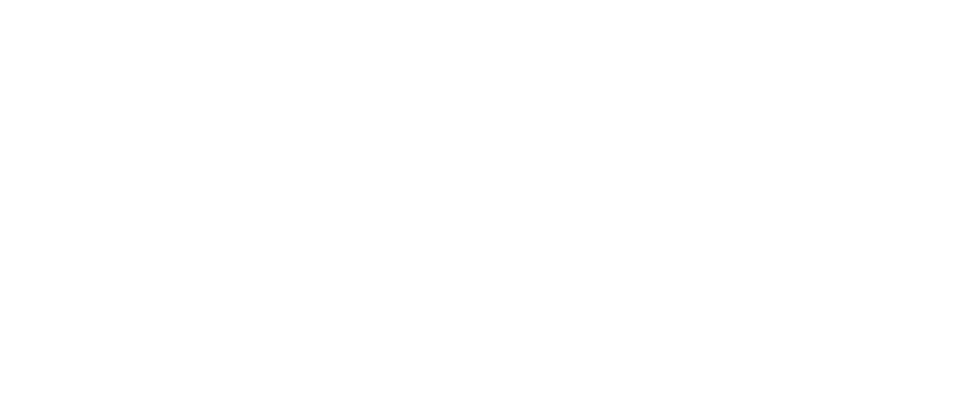
MOSFET half-bridge II
23.5.2003 So I burned whole driver board with my "skilful" :-(.
By a mistake I swapped 12 V with 35 V supplying in a chaos of wires from my power supply. Tantalum SMD blocking
capacitors was sticked into my table and MAX ICs was well damaged too.
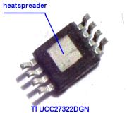
When I explored Internet I found some better MOSFET driver circuit - Texas Instrument
UCC27322, which gives 9A peak gate current. BTW its due to unique technology of combination bipolar and MOS transistors
in output stage. MOS is faster and bipolar have lower Uce drop in turn-on state and this lowers power loss.
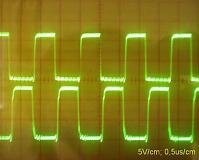
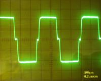
I decided to design my circuit and PCB from zero. 1st I made small comparison of last MAX5048 with new UCC27322.
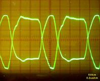
Both circuits had to drive 10 nF capacitor at 1 MHz. Oscillograms shows that UCC27322 produce faster rise time
(time resolution is 0,2 µs / cm). The circuit was made simply on test-board so longer connections
caused some ringing. I expect that on PCB it will be better.
 |
 |
 |
 |
| SMD package |
heatspreader |
MAX5048-10nF |
UCC27332-10nF |
UCC27322 IC have interesting metal facet at bottom of its package. Silicon chip is directly seated on it. It helps with
heat sinking out from a chip. When proper cooling plate is used UCC27322 can withstand 1,3 W power dissipation (compared
to 0,5 W of DIP-8 package)! So I tried to make large cooling copper plates and short power paths on new PCB layout. I placed
SMD tantalum and ceramic blocking capacitors everywhere. Because driver IC heats too much at 1,2 MHz I reinforced cooling
with copper plate pieces soldered on PCB. Also I use only 12 V instead allowed 15 V.
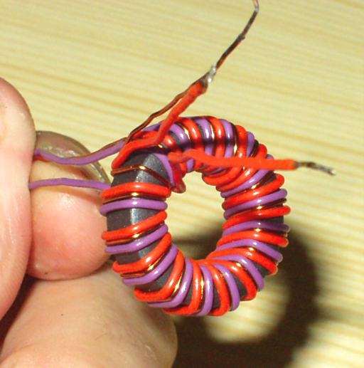
Then I rewound GDT trifilar 3x16 turns on new high quality ferrit core
Amidon FT 82-43
(d1 = 21 mm, d2 = 13 mm, h = 6,4 mm, Bmax = 0,275 T, µr = 850 - 3000 do 30 MHz)
which I bought in GES Electonic for 90Kč (about 2,6 euro).
(There's still old GDT on PCB photo).
Here is the schematic:
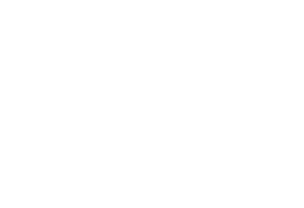
Function of this circuit is very similar to old circuit. I improved deadtime control.
Now four Schmitt inverters are used which has small own delay serving minimal deadtime. And they are shaping integrated
edge of square wave after RC circuit at NOR gate input (which is not Shmitt-like). Coming CLK signal with High level
is divided. One component go directly to input of NOR gate. Second component is delayed first and then go to other NOR
gate input. NOR gate output goes to Low immediately because only one active input is enough for it - see the truth table
below. After roll over CLK signal to Low there's still second NOR gate input held on High due to RC delay circuit for some
time and NOR gate output stay at Low. After RC delay elapsed (30 - 80 ns) NOR gate output turns High. This cause that
Low period is little bit longer than High period. The same situation is in other driver working with inverted CLK signal.
This mean that there cannot be overlay between roll over of both signals.
| A |
B |
non A |
OR |
NOR |
AND |
NAND |
| 0 |
0 |
1 |
0 |
1 |
0 |
1 |
| 0 |
1 |
1 |
1 |
0 |
0 |
1 |
| 1 |
0 |
0 |
1 |
0 |
0 |
1 |
| 1 |
1 |
0 |
1 |
0 |
1 |
0 |
 |
 |
 |
 |
| Uout UCC27322 |
Uout GDT |
Uout GDT-FETs |
Uout, Iout |
On 1st oscillogram can be seen the output voltage of both UCC27322 with no GDT connected.
(0,5 µs / cm). On 2nd one is GDT secondary voltage with no MOSFETs connected (0,2 µs / cm),
on 3rd one with connected MOSFETs. On 4th one is half-bridge output voltage and TC primary current. They should be
in phase with proper tune. When MOSFETs will switching in time while current passes zero (soft-switching) it would
lower switching losses significantly. I didn't tune it yet. Then I found that connecting TC primary via capacitor
which bring it to resonance is better than connecting it to capacitive divider with relative high capacitances.
1st I tested it with 35 VDC and 70 VDC power supply and then with variac (half-wave rectified,
100µF filtered). I got about 8 - 9 cm spark length with 150 V input voltage and 2,5 A
current draw. Sparks was very hot. When I tried to pull arc with screwdriver from secondary MOSFETs had blown.
I damage them a lot in further experiments. It is not cheap entertainment. It usually has shorted all three
electrodes and driver circuit drives this short. So I insert 400mA fast fuse into +12 V line to protect them.
Problems also occurred when I supply the driver from unfiltered power supply. There's some problems with PLL
synchronization. Maybe its filter or what? When circuit is out of tune the MOSFETs are stressed much more.
Or simply 1,2 MHz is too much for this electronic parts (hoping better future). I don't know anybody who
success at this frequencies. I saw this working at max. 400 kHz. But this wouldn't discourage me.
Maybe I will wound some bigger TC with lower fres...
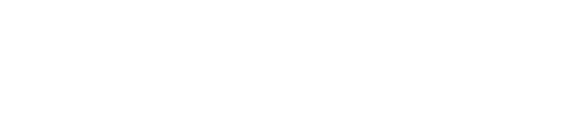
29.8.2003 I hadn't described details of connecting TC to half-bridge
above. So I would set it right now. There are three choices:
The first is interesting in that it doesn't use any primary coil. The output voltage from half-bridge is directly feed to
secondary base (base feed method). This have some advantages that we don't care about number of primary turns and coupling.
Also there is reduced flashover problem. And circuit is easier to analysis, see the theory.
Major disadvantage is relatively high impedance at resonance. It needs several kilovolts to be employed for driving and
this isn't easy to be done with nowadays MOSFETs. And the coil is galvanic connected to half-bridge power supply,
usually mains, that is dangerous.
In the middle is classic circuit (I have never seen anything else on foreign websites) which
using non-resonating primary coil. Second winding terminal is connected to the node of capacitive divider which removes DC
bias and makes RF filtering on power supply rails. Due to transformation effect the impedance in resonance is much lower
than in first case. Secondary winding is naturally insulated from half-bridge power supply.
The third circuit using resonating primary coil. There's a Cres capacitor in series with
primary winding. Its value is calculated to bring primary in resonance at same frequency as secondary fres. Then the impedance
is even lower than in second case. It allows to use lower voltage power supply or increase sparking with current power supply
(with enough powerful MOSFETs). It may interests foreigners from countries with 120V mains.
16.9.2003 Finally I decided to wind a new bigger TC with
lower self-resonating frequency. I hope to have less problems with semiconductors switching at lower freq. More about
BigTC here. Now I have TC with fres about 330 kHz. So I can buy more powerful MOSFETs now:
IRFP460 (500 V, 20 A, 250 W, 0,22 R). It had bigger gate capacitance of course. I think that my UCC27322 driving ICs would
burned at 1,2 MHz with this MOSFETs. But at 300 kHz are acceptable warm. New MOSFETs seems to be very robust because
I didn't burned them yet (knocking on the desk ;-). I also replaced serial diodes in MOSFETs sources with more powerful
Schottky diodes SR3060 (2 x 30 A).
Unfortunately there arose one big problem with PLL circuit. As
I was warned at HV-forum the xx4046 PLL's 1st comparator makes 90° phase shift when locked
properly! It explains mentioned phase shift on the previous oscillograms. So I tried to use
both remaining comparators in PLL IC but with no success. This comparators sets VCO to minimum frequency when input
signal is not present. I set 260 kHz. I also limited maximum frequency to 450 kHz by R-C network. The problem is that
PLL is refusing to lock while I'm doing with it everything I can. It produces fmin or fmax or locks at some wrong
frequency. If it occasionally locks (usually at high power supply voltage) at right frequency the lock is very unstable
and several frequency jitter can be seen. Also the phase is not perfect. Sound of sparks is strange squeaking and
random changing. When power supply voltage is significantly risen or lowered PLL unlocks. I tried to insert an inverter
between PLL and MOSFET driver board. I also tried to pickup feedback signal from current transformer at secondary base
instead from antenna but with no result.
I don't know why the first PLL's comparator lock so easily as well as with low power
supply voltage and other two not. I tried to make a bizarre circuit with two PLLs in cascade. I hope that both 90° phase
shifts would add to 180° and then I make a 360° shift by inverter. But it works only for very low power supply voltage.
With voltage rising the phase shift fast moved to about 90°.
In this moment I have no idea how to solve this. I'm asking you for help if you have
some experiences with xx4046 ICs or other PLLs.
 |
 |
 |
| 2 PLLs in cascade |
Upri vs Usec |
Upri vs Usec |
13.8.2004 I finally have a time to update my TC website
today. I will describe my advances with SSTC mostly from this year's winter time. Betweentimes my SSTC works quite
well for a few months. It reached streamers up to 38 cm long (running from 230 VAC mains). But read in sequence...
After many experiments with my current half-bridge PCB it seems to me proof enough
so I decided to make some nice housing for it. I don't like many things lying around because it increases probability
that something would accidentally touch together and blow up along time (experience by my own :-). I also put an
emphasis on good cooling and RF shielding. The base was made of 3 mm thick "L" shaped aluminium plate (bottom
and one side) which holds black profile of heatsink 12 x 10,5 x 3 cm making another side.
Opposite side holding control circuit is made of the same plate. The remaining side is made of alufoil-coated
(the inner side) wooden board. The top cover is not done yet because I often need to have access inside. The PCB is
mounted on spacers at bottom side of the box. Power transistors are oriented to face the heatsink side. To minimize
the thermal resistance between transistor's case and heatsink I used a kapton insulation pad that I bought in
GES. The pad is only 0,05 mm thick but it have dielectric strength 3,9 kV
and thermal resistance cca 0,53 K/W (for a TO-247 case). It's better than common silicone pad which has
Rth cca 0,7 - 1 K/W. Even better are insulation pads made of
Al2O3 ceramic
that can reach Rth down to 0,19 K/W at 1 mm thickness. To eliminate micro air gaps between transistor case
and heatsink I applied white silicone thermal-conductive pasta. On opposite side of transistor's case I mounted a
small aluminium "U" profile to improve cooling (like a sandwich) but most of heat is transferred through metal
back side. Anyway it may be a good protection against the transistor's case splinters during its explosion :)
Because of increasing the driver power I also replaced diode network around MOSFETs
using FYAF3004DN in series (fast Schottky diode 2 x 30A / 40 V in insulated TO-3PF case) and RHRP1560
parallel to MOSFET (hyperfast diode 15 A / 600 V, trr = 35 ns in TO-220 case). I mounted
the diodes on small heatsink mounted on bottom side of the box. Then I built in a linear stabilized power supply of
+5 V and +12 V for gate drivers and support circuits. To avoid a need of using variac I made a thyristor
pre-regulator modulating rectified mains voltage. It has also switched banks of filtering capacitors 220 µF
and 390 µF that may be used in any (parallel) combination or disabled. Mains voltage is filtered through
a line filter made of toroid ferrite choke and capacitor. Here's the result of my effort:
The thyristor pre-regulator uses 2N6509 (BT151 800R before) in classic phase controlled
rectifier circuit. There is also a single forward biased diode in series with thyristor that should stop a negative
voltage if thyristor would fail. The thyristor can be bypassed by a switch so then it will work as a simple half-wave
rectifier. Heating of thyristor during operation is minimal. This thyristor circuit also brings one big problem which
is implied from the principle of operation: the thyristor is turned on with 0 - 180° (in my case 30 - 170°)
phase delay in very short time. When the phase delay is set to 90° there is extreme dV/dt - voltage rise from
0 to +320 V within a few microseconds! But this is not acceptable for electrolytic filtering capacitors
and even the PLL circuit is unable to lock so fast. When I tested it first time I had attached a 10&micr;F elyt
capacitor and it became hot during very short time of operation. I catch up the power button in right time before
it could explode (I know that exploding capacitors are funny but it smells like a piss and made paper rubbish around
so I prefer to do it at school instead at home ;-). When a bigger capacitor would be used I guess it will kick off
mains fuse because of excessive current pulse. So the only safe way is to slow-down the rising edge of the pulse.
I used a big 250W choke from street lighting (with sodium lamps) that smooth the pulse to look like a half of sine
wave. The choke is not so small and light but still better than a variac. It didn't fit inside the box so I attach
it externally via cables. When there are no filtering capacitors attached to power rail it may cause a risk of
high voltage spikes so I connected a varistor in parallel. The choke also limits the peak current flowing through
half-brige. When I bypassed the choke MOSFETs blew out within a half of minute of operation. Here is the schematic
of power part of the driver:
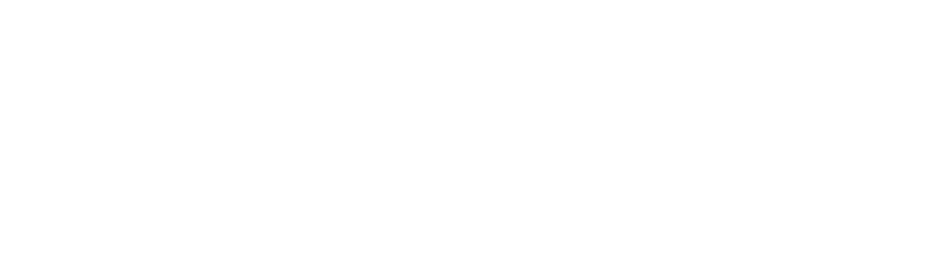
and controller part:
and some waveforms captured on thyristor pre-regulator without and with filtering:
 |
 |
| without Cf |
with Cf |
Further I had investigated the PLL circuit and came to surprising conclusion
that I measured output current wrong way all the time. Previously mentioned phase shift was caused by parasitic
inductive character of current sensing resistor that I used. I was trying to cancel phase shift that was never
existed. So it was not surprising that when I forced additional 90° phase shift into loop it stopped working.
Now I measure current via current transformer (that I grab from some old CRT monitor) terminated by 75Ω
non-inductive resistor. First I tried this measuring method with resistive load (a bulb and some hi-ohm resistors)
to prove it works well. Used CT is not superior but it's good enough to get some rough scope.
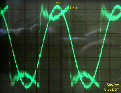
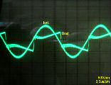
After connecting TC to the driver it seems that current and voltage waveforms are
OK and visible phase shift is quite small. When I manually tuned the PLL via variable resistor (voltage divider)
connected to VCOin (without feedback) it proved that the biggest sparks was reached on zero phase shift between
output voltage and current (that I seen as 90° before). But nothing is perfect and I can see that phase shift
is slightly varying with output power (resp. sparks length):
 |
 |
 |
| Uout, Iout |
Uout, Iout |
Uout, Iout |
So I left variable resistor there connected via 20kΩ resistor to VCOin
for phase shift fine tune. I set zero phase shift at maximum output power when it is most important. Maybe when I
would use current transformer at the bottom end of secondary coil to pick up feedback signal for PLL instead
of antenna it will be more stable but now I didn't get good results with CT.
audiomodulation
I got genius idea how to simply modulate TC output with low frequency signal.
I had already seen some "audio-modulated TC" on the Internet but it was made
quite a complicated way by modulation of power supply or using PWM modulation of the MOSFET bridge. But PLL
circuit is so challenging, it's just needed to couple a source of some audiosignal to VCOin input of the PLL.
And you don't need any extra power - a headphone output of common pocket music player is enough for deep
modulation of hundreds watts of RF power! This primary cause a frequency or phase modulation but due to the
fact that TC is a tuned resonator it will cause also amplitude modulation as a secondary effect. When driving
frequency is tuned away from f0 it will cause a significant drop of output power. When the driving frequency is
biased e.g. to the left side of resonant curve then positive modulation voltage will cause increase of driving
frequency which become closer to f0 and it will increase output RF power and negative modulation voltage will
cause decreasing of driving frequency which will be further from f0 and RF power will drop. What is the
purpose of this modulation? Such TC can be used as long/medium wave AM transmitter (proper antenna will
be needed for longer distance) or as a plasma tweeter. I was surprised how the audio-modulated sparks can
play quite well. It is similar to classic tweeter (missing bass) and it can be pretty loud. Signal distortion
depends on position of operating point on resonant curve - you have to bias it in the most linear segment.
It is done via variable resistor at VCOin that I mentioned before. During operation it can be also heard
a hissing noise of the sparks. If we would use high enough driving frequency (somebody says above 3 MHz)
then hissing noise will disappear and SNR will increase. Such high frequency can be achieved only with a very
small TC (a few centimeters dimensions) and its driving would be very difficult with common semiconductors.
There are available some special RF MOSFETs up to 30 MHz from IXYS
company but they are not cheap and not available in our country anyway. Have a look at
EasternVoltageResearch site, they are
developing such small TC called PlasmaSonic project. Here's a cut movie
(DivX 5.1; 1,86 MB taken by my digital camera Canon PowerShot A70)
of my audio-modulated TC playing Thunderstruck song from AC/DC :). I slightly overmodulated it to make spark
modulation more visible. But for small distortion it's needed to keep lower deep of modulation so visible
display will seem to be static. When I was trying audio-modulated TC first time I was fascinated by it and
spent some hours by playing various music via TC and I also successfully received my AM transmission on radio
placed in second room. Here's the final schematic of PLL circuit:
RF shielding is important:
You can see also a 74HCT04 inverter and jumper on the PCB that allows me to
choose inverted or non-inverted signal going from PLL but same effect can be achieved by swapping primary
coil terminals so it is not needed. I will mention the effect of inverted and non-inverted driving later.
I made a shielding box from 6 single-sided pieces of PCB soldered together. Before I made this shielding
there occurred an RF interference that drove my driver crazy. The top side is not hard-soldered but it's hold
by 2 wires and can be opened up. Antenna is simply made of 10 cm wire going through a small hole in
top side. On the right side is a jack connector for audio input and 3-wire cable (+5 V, GND, TTL signal
output) connected to driver base board.
The process of debugging MOSFET half-bridge was not painless. I blew off about
10 pairs of power MOSFETs. It happened in many cases: when I had detuned and unshielded PLL circuit, when I
tried to bypass filter choke in thyristor pre-regulator, when I tried to decrease the number of primary
coil turns and during my experiments with primary serial resonant capacitor.
During my previous experiments I connected TC primary coil without resonant
capacitor - cold primary terminal was attached to the middle node of 1µF film capacitor divider between
power rail and ground. In this case I got only up to 20 cm long sparks to grounded object while RMS
power consumption was around 200 W. When I connected electrolytic filter capacitor to power rail sparks
became much shorter but very hot and it was melting the iron spike of discharge electrode. RMS power consumption
was increased to around 300 W. Power MOSFETs was only slightly warm so I though that I should decrease the
number of primary turns (lower impedance) to increase power and prolong the sparks. I tried it twice but both
experiments quickly ended with death of MOSFETs (even I didn't observed any significant warm up) and spark
length didn't prolonged. So it seems this is not the right way to go. Here's a photo of some of semiconductors
that died during my experiments. BTW I observed that fuse in mains circuit is just for fun because in 90% of
cases it blew together with MOSFETs (simply coz it's too slow) sometimes together with clap of mains circuit
breaker on the wall. Sometimes it scattered to little pieces and I had to shake out all this garbage
from fuse holder.
Silicon Heaven
Further I mostly used tuned primary coil. On foreign sites this idea was
spread too under the name DRSSTC (Double Resonant Solid State Tesla Coil).
I would say that my DRSSTC was one of the firsts, constructed in August 2003. So primary coil is in
series with a resonant capacitor which tunes primary circuit to the same frequency as the secondary f0.
It's good idea to tune primary circuit slightly below secondary f0 because of f0 will drops when sparks
appears and become larger. Due to resonance the voltage on primary coil (and capacitor too) will rise to
thousands volts and also will transform to higher voltage on secondary side. Resonant capacitor must
be robust with low ESR and ESL because of huge current is flowing through it. In my first experiment
I used some small disk ceramic capacitors which had been burnt within 10 seconds. I found that high
voltage (usually a few nF at 1500 - 2000 V) pulse film capacitors from a CRT TV or monitor deflection
circuit works very well. There are available WIMA FKP1 pulse capacitors in GME
but they are quite expansive (about 30,- CZK per one) so a serial-parallel network forming a MMC will cost
a lot. Currently I use parallel combination of 5,6 + 5,6 + 0,47 nF (11,6 nF together)
to make primary resonate at 340 kHz. The effect of scattering resonance into 2 peaks due to high
coupling has occurred here. Lower peak is at 290 kHz and higher peak is at 405 kHz. It's interesting
that I got much longer fatter and straight sparks at higher 405kHz peak. On lower peak the sparks are more
weak, forked and makes little bit cracking sound instead pure 50Hz hum which indicated bad tuning.
I can switch between this 2 peaks by including or bypassing an inverter on PLL output or just swapping
primary leads on half-bridge output. I don't fully understand this effect yet...
In this DRSSTC mode I reached 35 - 40 cm long sparks but
also the power consumption and power dissipation has rose significantly (up to 800 W without filter
caps.). After a few minutes of run time the heatsink temperature reach about 60°C and also the
same for resonant capacitor. Even the primary coil wire with 2mm diameter will warm up. But I don't
need to run TC on full power for a long time. Maybe I should mount some fan on the heatsink. Here is a
table of real power consumption (measured with TrueRMS wattmeter DMM Metex M-3860M, thyristor
pre-regulator is fully opened so it equals to half-wave rectifier, 230 V mains voltage) of whole
driver in dependence of configuration:
| SSTC |
DRSSTC |
supply filtering |
| 197W |
645W |
without filter cap., only choke |
| 217W |
850W |
without filter cap., without choke |
| 288W |
960W |
with 220µF filter cap. and choke |
| 495W |
- |
with 220µF filter cap., without choke |
By using a variac I tried to measure how the spark length depends on total input power:
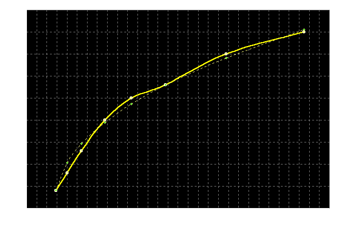
This curve roughly match a square root function. I tried to estimate an empiric function
(dashed line) for spark length: l = k*(P-P0)q, [cm; W]
with parameters k = 1,7; q = 0,46 and P0 = 110. If a full-bridge
would be used instead of a half-bridge, then voltage and current swing will be 2x more and power
will be 4x more but sparks will be only rougly 2x longer. Need to say that spark length also depends
on other factors like duty cycle, modulation waveform, toroid, etc. So this measurement can be seen
only as relative, valid for one specific SSTC.
IGBT half-bridge
 15.8.2004 Now I would like to introduce a new progressive semiconductor
switching part - an IGBT transistor. This shortcut stands for Insulated Gate Bipolar Tranzistor.
This means it behaves like a common bipolar transistor at output but has an insulated gate so
behaves like a MOSFET on input. IGBT is not a hot new part. I have known about it for a long time
but I saw mostly the extreme power IGBT bricks which are too slow and so they are useless for
driving my SSTC. Recently when I browsed Fairchild
semiconductors product list and datasheets I had discovered a few smaller IGBTs with pretty good
dynamics parameters which can compete commonly used MOSFETs for building a SSTC. IGBTs combine
advantages of both MOSFETs (controlling by electric field instead of pushing huge base current)
and bipolar transistors (low saturation Vce voltage - less static power dissipation). When
switching higher currents usually the Vdrop on MOSFET caused by its Rdson exceed Vces so
IGBT has less power dissipation than MOSFET. And when the junction temperature would rise
the Rdson of MOSFET will rise too but the Vces of IGBT will drop. For example let's compare
MOSFET IRFP460 (Vdsmax = 500V, Id = 20A, Rdson = 0,27 R) and
IGBT FGH20N6S2D (Vcemax = 600 V, Id = 28 A, Vces = 2,5 V @14 A)
so static power dissipation of the MOSFET will be 53 W at Id = 14 A (3,78 Vds drop)
and power dissipation of the IGBT will be only 35 W. IGBTs are more robust and can handle
larger peak current. Some of them are short circuit rated - this means that IGBT can short
power supply rails and withstand the short circuit current for some microseconds (time depends
on Vge, harder driving - less time). Another big advantage of IGBTs is that its structure
doesn't include any body diode between collector and emitter like inside MOSFETs.
So then manufacturer can implement inside a hyperfast recovery diode (trr about 35 - 70 ns)
or let users to connect any other external diodes. This simplifies bridge structure and
also decreases parasitic inductance caused by needed additional wiring around MOSFETs.
Gate capacitance of an IGBT is similar or maybe less than Cg of comparable MOSFET. Rated Vge is
typically ±20V (±30V pulse). Threshold gate voltage is ussually bigger than for
MOSFETs. Dynamics parameters of new IGBTs are quite good. It's interesting that most of
IGBTs has significantly (many times) longer toff_delay compared to ton_delay
(e.g. 55 / 13 ns). This asymmetry prolongs the cross conduction (while low-side
IGBT turns on very fast then high-side IGBT still stays turned on for some time and vice-versa)
when a huge current is flowing from supply rail to groud through both IGBTs (if there's not
enough deadtime). On the other side short circuit rated IGBTs shouldn't have a problem
to withstand this cross conduction current for some tenths of nanosecons but it increase
power dissipation. Here's my working table with comparison
of important parameters of some IGBTs and MOSFETs which I studied.
15.8.2004 Now I would like to introduce a new progressive semiconductor
switching part - an IGBT transistor. This shortcut stands for Insulated Gate Bipolar Tranzistor.
This means it behaves like a common bipolar transistor at output but has an insulated gate so
behaves like a MOSFET on input. IGBT is not a hot new part. I have known about it for a long time
but I saw mostly the extreme power IGBT bricks which are too slow and so they are useless for
driving my SSTC. Recently when I browsed Fairchild
semiconductors product list and datasheets I had discovered a few smaller IGBTs with pretty good
dynamics parameters which can compete commonly used MOSFETs for building a SSTC. IGBTs combine
advantages of both MOSFETs (controlling by electric field instead of pushing huge base current)
and bipolar transistors (low saturation Vce voltage - less static power dissipation). When
switching higher currents usually the Vdrop on MOSFET caused by its Rdson exceed Vces so
IGBT has less power dissipation than MOSFET. And when the junction temperature would rise
the Rdson of MOSFET will rise too but the Vces of IGBT will drop. For example let's compare
MOSFET IRFP460 (Vdsmax = 500V, Id = 20A, Rdson = 0,27 R) and
IGBT FGH20N6S2D (Vcemax = 600 V, Id = 28 A, Vces = 2,5 V @14 A)
so static power dissipation of the MOSFET will be 53 W at Id = 14 A (3,78 Vds drop)
and power dissipation of the IGBT will be only 35 W. IGBTs are more robust and can handle
larger peak current. Some of them are short circuit rated - this means that IGBT can short
power supply rails and withstand the short circuit current for some microseconds (time depends
on Vge, harder driving - less time). Another big advantage of IGBTs is that its structure
doesn't include any body diode between collector and emitter like inside MOSFETs.
So then manufacturer can implement inside a hyperfast recovery diode (trr about 35 - 70 ns)
or let users to connect any other external diodes. This simplifies bridge structure and
also decreases parasitic inductance caused by needed additional wiring around MOSFETs.
Gate capacitance of an IGBT is similar or maybe less than Cg of comparable MOSFET. Rated Vge is
typically ±20V (±30V pulse). Threshold gate voltage is ussually bigger than for
MOSFETs. Dynamics parameters of new IGBTs are quite good. It's interesting that most of
IGBTs has significantly (many times) longer toff_delay compared to ton_delay
(e.g. 55 / 13 ns). This asymmetry prolongs the cross conduction (while low-side
IGBT turns on very fast then high-side IGBT still stays turned on for some time and vice-versa)
when a huge current is flowing from supply rail to groud through both IGBTs (if there's not
enough deadtime). On the other side short circuit rated IGBTs shouldn't have a problem
to withstand this cross conduction current for some tenths of nanosecons but it increase
power dissipation. Here's my working table with comparison
of important parameters of some IGBTs and MOSFETs which I studied.
Because The MOSFETs in my DRSSTC driver are very heavily loaded
I decided to replace it by IGBT FGH50N6S2D (Vcemax = 600 V, Id = 75 A,
Uces = 1,9 V @30 A, Qg = 70 nC @15 V)
which easily overpowers used IRFP460 (quite obsolete) MOSFET in all parameters. Gate driver
circuit and GDT didn't need to be changed. I just replaced the transistors. DRSSTC started
without any problems. It seems to me that IGBTs are slightly less heating. Also sparks was
prolonged by few cm (and power consumption has increased - up to 850W without elyt filter
capacitors). But at the same time I raplaced resonant capacitor too so it may be rather affected
by this. I measured current draw of the whole driver circuit and it was 170 mA with zero
voltage over IGBT's power rail and 217 mA under full load at 380 - 400 kHz.
Just for a test I tried to measure heatsink warm up within
90s on full power. I used digital temperature sensor Dallas DS18B20 placed in a hole in
heatsink near 2 cm from IGBT case connected to PC (BTW Dallas 1-wire bus proved a good
noise imunity against the radiated field from TC :). Heatsink temperature had risen from 30°C
ambient temperature to 45°C (maximum occurred after some delay after shut down due to thermal
inertia). So temperature difference is 15°C and I calculated heatsink thermal capacitance
to be 388 J /°C. This means that IGBTs must heated 65 W or more.
But I don't know how much heat was radiated away so this calculation doesn't give much
sense :-\
Here are some oscillograms of high side MOSFET gate voltage
(2 on the left side) and high side IGBT after replacement (2 on the right side). One is taken
for minimal power when PLL is not locked yet and other is for max. power.
 |
 |
 |
 |
| Ugs, min.power |
Ugs, max.power |
Uge, min.power |
Uge, max.power |
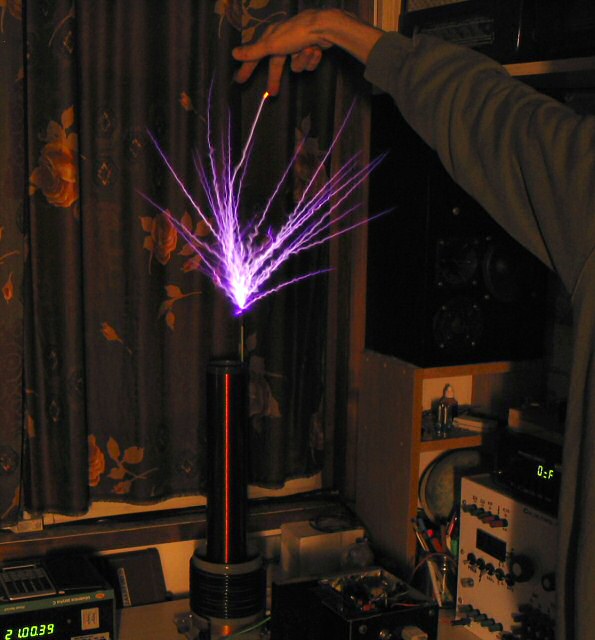
And finally here are some photos of streamers. The 1st photo on left
is without the resonant primary capacitor, next are with Cres. All on full power. And one sparky
movie (DivX 5.1; 176 kB). As a further project I plan to
build a full-bridge with four FGH60N6S2 IGBTs and with some smarter driving circuit.
8.8.2005 Now I have powerful HV/HF supply
so I decided to build a homemade Geisslerovu tube.
Very simple and quick experiment can be done with an old glass syringe that we choke by wet finger
and pull out the piston so low pressure area is created inside the cylinder. Then we put it in RF field
around top of CW running tesla coil. If there's sufficient intensity you will see glowing discharge
inside. I don't suggest to try this with a plastic syringe because it will melt and you get RF burns to
your fingers from the discharge. It worked for me on the first try but I would like something bigger.
I chose an elongated glass from olives (height about 14 cm).
I drilled a hole through the metal cap and soldered a piece of copper pipe inside. One electrode
was made from a needle spike soldered to inner side of the cap. Second electrode is freely lying
at the bottom of the glass (capacitive coupling only). It's made of a small screw with grinded
spike and washer that stabilizes it in position where spike is directed oposite to top electrode.
I connected the copper pipe protruding from the cap to intake of a compressor from an old fridge by
a piece of short hose. Output of the compressor was going to another glass with water. I turned
on the compressor and I was waiting untill bubbling in water disappear. I have no idea what level
of depression was there because I don't have equipment to measure it. Then I strongly pressed the
hose by tongs and pulled out one end from compressor intake pipe and stuffed it by a metal roller.
There's a risk of sucking outer air inside the glass during this operation. I tried it more times
until I was satisfied with the result. When I put the bottom of the glass close to top of running
tesla coil the glowing discharge was ignited between two electrodes inside. After 2 weeks the discharge
became little bit weak and after some months I was unable to ignite the discharge in full length of
the glass. I am aware that it cannot be fully hermetical. This would require some glass-work and
solve a sealing of evacuated tube...
10.11.2008 I put my DRSSTC half-bridge driver
with IGBTs under heavy load on last Teslathon 2008. After longer pulling of arcs
to a light bulb a blackout of the room has suddenly occurred. Fuse on the house switchboard was blown
but I wonder that small T 6,3 A fuse in the driver survived. I though that IGBTs died but after some
later measurement at home I found that only protective varistors on main bridge supply rail was cracked.
Diodes in tyristor preregulator died too due to the short circuit. I replaced the cracked varistor pair
by three bigger (4,5 kA peak current rated) varistors from
Semic.
When I checked availability of used IGBTs FGH50N6S2D and FGH60N6S2 by
Fairchild I found out that this IGBTs became obsolete. A last few pieces can be bought from
Farnell
and Arrow. So I sent a question
to Fairchild tech. support asking for some suitable replacement of these IGBTs and they suggested me
HGTG30N60A4, HGTG40N60A4, FGH60N60SF. But I was disappointed by large total gate charge and long turn
off delay (see table bealow) compared to older ones. This may be a problem for high frequency switching.
They told me that new IGBTs has lower Eon and Eoff energy than older ones. But I guess that in
a bridge topology circuit it is much more important the matching of switching times tdon, tr, rdoff,
tf to minimize cross-conduction time. I also asked Starmans Electronics
distributor and they recommended me IXGH40N60C2D1 alternative by IXYS for a quite good price 149,- CZK
inc. VAT. So I just bought 2 IXGH40N60C2D1 for testing and backup. But I would state that old good
FGH60N6S2 cannot be overpowered by any of this replacements. Here's a list of important parameters
of discused IGBTs:
| IGBT type |
Uce [V] |
Uces [V] |
Ic [A] |
Pd [W] |
Qg [nC] |
tdon [ns] |
tr [ns] |
tdoff [ns] |
tf [ns] |
D-trr [ns] |
| FGH50N6S2D |
600 |
1,9 |
75 |
463 |
70 |
13 |
15 |
55 |
50 |
50 |
| FGH60N6S2 |
600 |
1,9 |
75 |
625 |
140 |
18 |
15 |
70 |
50 |
- |
| HGTG30N60A4 |
600 |
1,8 |
75 |
463 |
225 |
25 |
12 |
150 |
38 |
- |
| HGTG40N60A4 |
600 |
1,7 |
75 |
625 |
350 |
25 |
18 |
145 |
35 |
- |
| FGH40T65SHDF |
650 |
1,5 |
80 |
268 |
68 |
18 |
27 |
64 |
3 |
100 |
| FGH40N60SMD |
600 |
1,9 |
80 |
349 |
119 |
15 |
22 |
116 |
16 |
36 |
| FGH60N60SF |
600 |
2,3 |
120 |
378 |
198 |
22 |
44 |
144 |
43 |
- |
| IXGH40N60C2D1 |
600 |
2,0 |
75 |
300 |
95 |
18 |
20 |
90 |
32 |
100 |
| C2M0080120D SiC FET |
1200 |
80 mΩ |
31 |
208 |
49 |
12 |
14 |
23 |
18 |
40 |
Uces, Ic, Pd, txx @25°C, Uces @ 40A, trr @30 A, Qg @15 V
In the near future there will be available an interesting alternative:
IGBT transistors made of silicon carbide (SiC).
They are faster, has lower Vces, doesn't suffer by deep saturation and can work at higher temperatures.
It woulde be possible to reduce power losses more than 50% by simple replacement but currently there are
only few models available for high prices.
17.12.2013 UPDATE: good days are comming,
prices of SiC semiconductors dropped significantly. I just found a new SiC 1200V power MOSFET
C2M0080120D
by Cree (see the last line of the table above) that is available on Digikey
for 16,67 $ or Mouser
for 13,33 euros. This prices are similar to fast silicon IGBTs. This FET offers devil speed with
low driving gate power requirement. I guess that running a 1MHz bridge would be easy with it. The
only one problem of this SiC FET is assymetric gate drive max. -10 / +25 V. This disable an
easy way of direct gate driving via GDT. To fully open the device it requires at least 16 - 20 V
gate voltage.
24.12.2008 I decided that I should make
some better discharge terminal for my BigTC and replace that piece of wire
by something with a better look. I remember that I saw using of a sparking-plug on some foreign
website years ago. So I cleaned the sparking-plug, ground away all sharp edges and polished the
metal surface. Then I mounted it on a plexiglass circlet and glued it inside on top of secondary
PVC pipe. Sparking-plug body is connected with a short piece of wire to hot end of secondary winding.
There's a M4 screw on top of sparking-plug. I screwed on a piece of metal tube with internal threading
so I can screw on various metal spikes. When the spike will be burned by strong arcing I can
replace it easily. I also tried an ion-motor made as a 4-tail star cut from metal sheet with
crooked tails, which I put on the spike of new discharge terminal. During a short time it will
rotate at high RPMs. I'm afraid of it could jump off the small dinge and fly away :). New terminal
is also more robust so it's easy to put a toroid on it.
Some time ago I found a small plastic toroid (probably a boat bumper)
during a walk. I wrapped it carefully by aluminium foil and put on top of my TC. That toroid with
polystyrene body I used before was not so good - it became to collapse due to heat produced by RF
currents. This one is made of tough plastic so it should withstand it. Resonant frequency was
dropped by 50 kHz. Arc length was not prolonged significantly but sparks became fatter and
also it hurts more when touched by hand. IGBTs are not much happy with this and produce more heating
so it's not suited for longer run time.
20.8.2012 A small accident has happened
to my SSTC during summer Teslathon 2012. After about 1 minute of happy
sparking a white smoke appeared coming out from the power box. I turned it off and blew out the smoke.
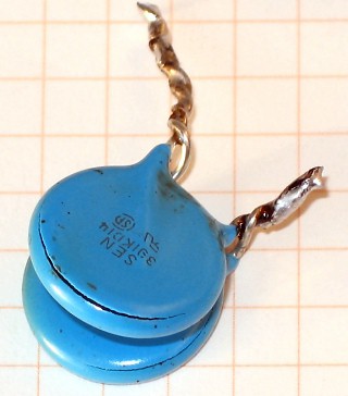
I saw that it was leaking out of film capacitor Tesla TC207
1 µF / 400 V used in C-divider for power rail blocking and AC coupling the
output of half-bridge. Now I know that this TC207 class of capacitors are not good for handling RF
and high currents. I replaced it by some more powerful caps 5 µF / 400 V.
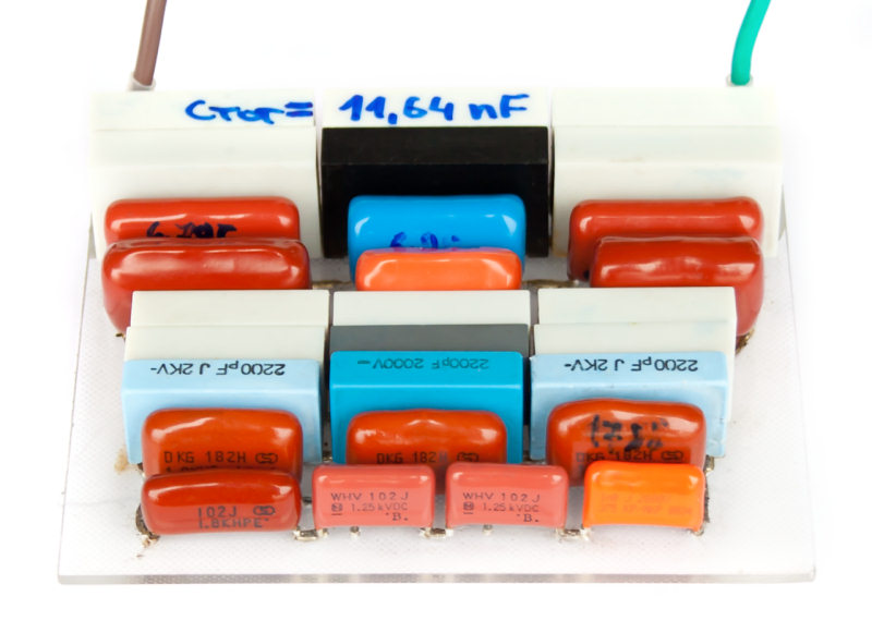
I also reworked the resonant capacitor to look better. I made new MMC on a piece of plexiglass.
I used mostly polypropylene impulse capacitors Tesla TC344
that I formed into 9 parallel strings, each of 3 capacitors (min. 1600 VDC rated) in series
(4800 VDC total rated). I tried to slightly vary the capacity of MMC and ended with 11,64 nF
(this is very close to old value). The MMC is not heating during operation.
Later during playing with a toroid on secondary I accidentally flip
the switch for bypass thyristor pre-regulator that resulted in damage of IGBT pair FGH50N6S2D,
R.I.P. they worked for along time and very well, but you know this IGBT = It Goes Bang Too :)
I replaced it by my last stocked pair of IGBT FGH60N6S2
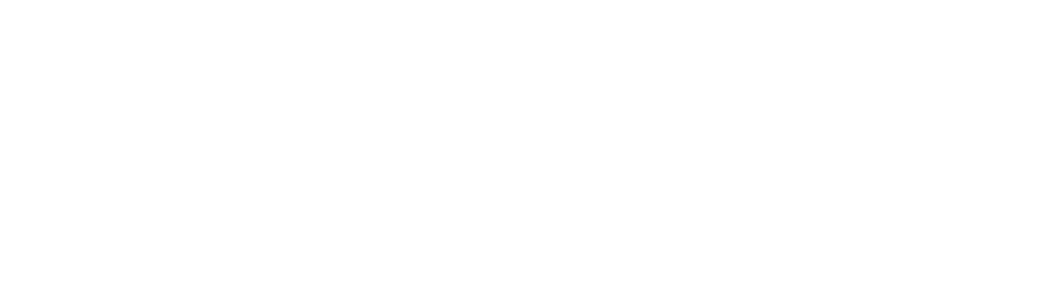
without internal diode. I also replaced external diodes by faster Vishay VS-30ETH06FP
(600 V / 30 A / 30 ns) and bypassed schottky diodes connected in series with power transistors.
They were used to disable MOSFET's internal body diodes but now when I use IGBTs they are no longer needed.
Here is updated schematic of power part of the SSTC circuit: